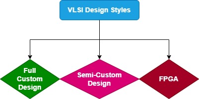
VLSI Design Styles
PLEASE CLICK ON THIS LINK TO SEMI-CUSTOM DESIGN ASIC
Full Custom Design:
Despite its challenges, full custom design is still widely used in many industries, including the semiconductor and microelectronics industries, where it is often necessary to create highly optimized and customized circuits for specific applications.
PLEASE CLICK ON THIS LINK TO SEMI-CUSTOM DESIGN ASIC
Semi-Custom Design:
In VLSI (Very Large Scale Integration), semi-custom design refers to the process of designing an integrated circuit (IC) using pre-designed and pre-verified building blocks or cells, which are combined to create a custom circuit.
In semi-custom design, the designer uses a library of pre-designed cells such as gates, flip-flops, and other combinational and sequential logic elements to create a custom circuit. The pre-designed cells are typically characterized for performance, power consumption, and other design metrics, which allow the designer to select the best cells for their design based on their requirements.
Semi-custom design can significantly reduce the time and effort required to design a complex IC, as the designer does not need to start from scratch, but rather can use pre-verified building blocks to create the desired circuit. This approach is often used in the design of digital circuits such as microprocessors, memory, and application-specific integrated circuits (ASICs). However, it may not be suitable for all types of designs, and some circuits may require a fully-custom approach to achieve the desired performance and functionality.
FPGA - Field Programmable Gate Array:
FPGA stands for Field-Programmable Gate Array. In VLSI (Very Large Scale Integration) design, an FPGA is an integrated circuit that can be programmed and configured by the user after manufacturing. It is a reprogrammable logic device that allows designers to create custom digital circuits without having to build a custom ASIC (Application-Specific Integrated Circuit).
FPGAs contain a large number of programmable logic blocks, configurable I/O (input/output) blocks, and programmable interconnects that allow users to create complex digital circuits. Users can configure the FPGA using a hardware description language (HDL) such as Verilog or VHDL. Once the design is complete, the configuration file is loaded into the FPGA, which then behaves as if it was designed for that specific application.
FPGAs are used in a wide range of applications, such as digital signal processing, aerospace and defense, medical devices, and industrial automation, among others. They are particularly useful for prototyping and testing new digital circuits and systems, as well as for low-volume production runs.

Comments
Post a Comment